Vsd Intern - Dac Ip Design Using Sky130 Pdks - Part 1
Posted on 12 Dec 03:08 | by mitsumi | 8 views
Last updated 5/2021
MP4 | Video: h264, 1280x720 | Audio: AAC, 44.1 KHz
Language: English | Size: 704.25 MB | Duration: 1h 45m
Overview of DAC Theory, Circuit and project flow
MP4 | Video: h264, 1280x720 | Audio: AAC, 44.1 KHz
Language: English | Size: 704.25 MB | Duration: 1h 45m
Overview of DAC Theory, Circuit and project flow
What you'll learn
Overview of DAC
Background and Principle of Operation
Implementation Aspects and Challenges
Evaluation Parameters
Expected Input Output Characteristics
Requirements
VSD - Circuit Design and SPICE simulations
VSD - Custom Layout
VSD Intern - Bandgap IP Design
Description
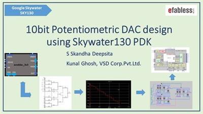
The webinar aims to design a 10-bit potentiometric Digital to Analog Converter using end-to-end Open-source EDA tools. The target is to design 10-bit potentiometric DAC with 3.3v analog voltage, 1.8v digital voltage and 1 off-chip external voltage reference using sky130nm technology node.In real world, most of the data available is in the form of analog in nature. We have two types of converters analog to digital converter and digital to analog converter. These two converting interfaces are essential to obtain the required operations of a processor to manipulate the data of digital electronic equipment and an analog electric equipment. Digital to Analog Converter (DAC) is a device that transforms digital data into an analog signal in order to interact with the real world. The digital signal is represented with a binary code, which is a combination of bits 0's and 1's. The digital data can be produced from a microprocessor, Field Programmable Gate Array (FPGA), or Application Specified Integrated Circuit (ASIC). There are two commonly used DAC conversions – Weighed resistors method and R-2R ladder network method. Applications of a DAC: audio amplifier, video encoder, display electronics, data acquisition systems, calibration, Digital potentiometer.This webinar will cover1) Overview of DACWhy DAC?Background and Principle of Operation.Implementation Aspects and Challenges.Evaluation Parameters.2) Project Design Specs and DAC CircuitCircuit BehaviourExpected Input Output Characteristics.3) Project Flow –Analog IP – Hands-onFlow of Steps for Analog IP design.Tools RequiredSetup of ToolsLibraries Requirede) Setup and linking Libraries.All the best and happy learning
Overview
Section 1: Introduction and DAC Overview
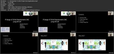
Lecture 1 Introduction To DAC Project And Applications
Lecture 2 Background And Principle Of Operation
Lecture 3 Reference Voltage Resolution And Linearity Aspects Of DAC
Lecture 4 Monotonicity, Settling Time And Speed Of DAC
Section 2: DAC Specs, Implementation Aspects and Challenges
Lecture 5 DAC Architectures, Applications, Decoding Method And Switching Network
Lecture 6 DAC Non-Linearity And Output Voltage Level Parameters
Lecture 7 DAC Interface Specs And Operating Modes
Lecture 8 DAC DNL and INL Specs
Section 3: 10-bit DAC Implementation strategy
Lecture 9 Fundamental DAC Circuit
Lecture 10 10-bit DAC Implementation Strategy - Divide And Conquer
Lecture 11 From 2-bit DAC to10-bit DAC
Section 4: Tool Setup steps
Lecture 12 Detailed Steps To Install Latest NGSpice From Scratch
Lecture 13 Detailed Steps To Install And Configure Magic With Sky130 PDKs
Lecture 14 Detailed Steps To Install And Configure Xshem With Sky130PDKs
Lecture 15 Simple Inverter Design Using Xschem And Sky130 Models to confirm tool install
Lecture 16 Simple Pre-Layout Simulation Steps Using NGSpice
Section 5: Conclusion
Lecture 17 Conclusion
Curious freshers looking to enter into analog and mixed-signal VLSI design,Beginner or Professional Physical Design Engineers looking to know more about IPs and Macros
Download link
rapidgator.net:
uploadgig.com:
[/b]:
[b]1dl.net:
Related News
System Comment
Information
 Users of Visitor are not allowed to comment this publication.
Facebook Comment
Member Area
Top News

